



MOSFET Transistors
MOSFET transistors for hi-rel applications: N-channel types in a hermetic ceramic package, rated -55 °C to +150 °C and screened to a programme patterned after MIL-PRF-19500. For switching and signal tasks in aerospace, defence and instrumentation.
|
|
||||||||||||
|---|---|---|---|---|---|---|---|---|---|---|---|---|
| OPTEK Technology | N-Channel | 1 | Enhancement | 60 V | 75 mA | 100 mS | 10/10 ns | 3 | Yes | -55 °C | 150 °C | |
| OPTEK Technology | N-Channel | 1 | Enhancement | 60 V | 75 mA | 100 mS | 10/10 ns | 3 | Yes | -55 °C | 150 °C |
Our
manufacturer
Brochures
Here you will find bundled information on the topic as well as selected brochures with further content, technical background information, and practical solutions.

Frequently asked questions about
MOSFET Transistors
The questions on this page come from conversations with engineers designing a component in and with buyers who need to replace an existing type. They range from the basics to the details that show what really matters during selection. Whatever remains open we clarify for your specific case: tell us your target values – we narrow down the eligible series and give you price, availability and samples for your quantity.
02
How do you drive an enhancement mode MOSFET correctly?
An enhancement mode MOSFET is only driven reliably well above its threshold voltage VGS(th) — just above it the device conducts, but not at the channel resistance quoted in the datasheet. The range given there is a device-to-device spread, not an operating point: the HCT7000 series specifies 0.8 to 3.0 V (VDS = VGS, ID = 1 mA). Design against the upper end, and verify safe blocking against the lower one.
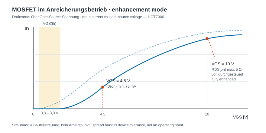
The channel is only fully enhanced well above that. The datasheet guarantees RDS(on) of 5 Ω at VGS = 10 V, whereas at VGS = 4.5 V it only guarantees an on-state drain current ID(on) of at least 75 mA. Driving from a 3.3 V or 5 V logic level therefore means either accepting the higher channel resistance or adding a gate driver. The forward transconductance Gfs of 100 mS applies at VDS = 10 V and ID = 0.2 A.
03
What do the TX and TXV suffixes mean on hi-rel transistors?
TX and TXV identify the screening level, not different electrical behaviour: an HCT7000MTX is the same transistor as an HCT7000M, just additionally tested. The scheme comes from MIL-PRF-19500, the US general specification for discrete semiconductors, which distinguishes the quality levels JAN, JANTX, JANTXV and JANS. TX adds screening tests on every individual device, TXV adds pre-cap internal visual inspection of the die before the package is sealed.
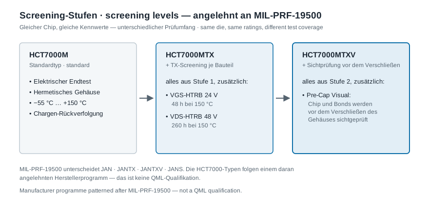
For the TX and TXV types of the HCT7000 series, OPTEK states a screening programme patterned after MIL-PRF-19500, with a VGS HTRB at 24 V for 48 hours at 150 °C and a VDS HTRB at 48 V for 260 hours at 150 °C. The wording matters for procurement: "patterned after" is not the same as JAN qualification on the QML. Where a qualified part is required, the level belongs explicitly in the specification.
04
Which parameters decide the choice of a MOSFET?
Six quantities decide it — and for each of them the test condition under which it applies:
- VDSS, the drain-source breakdown voltage, dimensioned with headroom for switching overshoot
- ID and the permissible power dissipation PD, which in practice usually limits the design before the current rating does
- RDS(on) — always together with the VGS at which it was measured
- VGS(th) as a spread band, which decides logic-level compatibility
- Ciss, Coss, Crss plus t(on) and t(off) for driver effort and switching losses
- Thermal resistance RthJC and RthJA together with the maximum junction temperature
The test condition is not a footnote: on the HCT7000 series, RDS(on) and VDS(on) are specified at 0.5 A, above the continuous rating of 200 mA — a pulsed measurement, not a permissible operating point. Taken into a dissipation calculation unchecked, it points at an operating case the device does not allow.
In a hi-rel context two non-electrical criteria are added: the package style including hermeticity, and the required screening level. Neither can be retrofitted later.
05
Why do hi-rel MOSFETs come in a hermetic ceramic package?
A hermetic package permanently separates the die from the surrounding atmosphere, whereas plastic moulding lets moisture through — that is the reason for this package style. The properties for which it is chosen in hi-rel design follow from it:
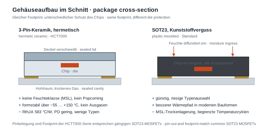
- No moisture uptake and therefore no moisture sensitivity level, no dry storage, no popcorning during reflow
- Dimensional stability across many temperature cycles between -55 °C and +150 °C
- No outgassing of moulding compound under vacuum
The price for it is in the datasheet as well: the thermal path is poorer than in modern surface-mount power packages — RthJA is 583 °C/W — the permissible dissipation is correspondingly low, and the range of types is small. A hermetic package does not replace thermal design, it only shifts the failure mechanism.
06
How is a MOSFET thermally designed and derated?
The permissible dissipation is calculated back from the thermal resistance and the maximum junction temperature rather than taken from the headline figure: Pperm = (Tj,max - Tambient) / Rth. For the HCT7000 series with Tj,max of 150 °C and RthJA of 583 °C/W, roughly 214 mW remain at 25 °C ambient, about 111 mW at 85 °C and only about 43 mW at 125 °C. With a defined heat path through the case, RthJC of 100 °C/W applies instead — and then the datasheet value of 600 mW is the limit.
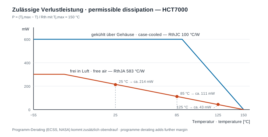
Hi-rel projects add a second stage: derating rules from programme standards such as ECSS-Q-ST-30-11 or NASA EEE-INST-002 require further margin against the voltage, current and temperature limits. Which factor applies is defined in that standard and in the programme handbook, not in the component datasheet.
07
In which applications are hi-rel MOSFETs worthwhile – and when are they not?
Hi-rel MOSFETs are worthwhile wherever replacement costs more than the component: in aerospace, defence electronics, medical technology, downhole and process instrumentation, and in long-life systems where an unannounced manufacturing change would trigger requalification. Typical tasks are signal and small-load switching, level shifting, driving relays and optocouplers, and analogue switching.
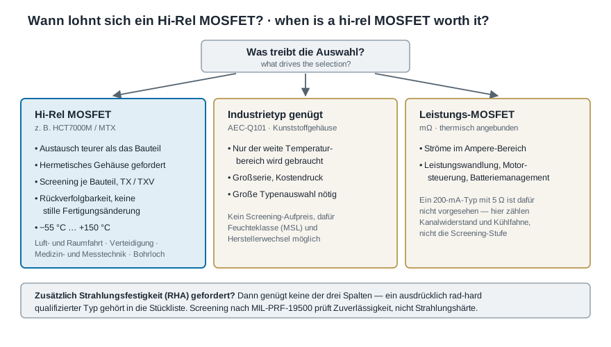
They make little sense in two cases. First, in genuine power conversion: for motor control or converters in the ampere range, types with milliohm channel resistance and a thermally bonded power package are the right choice, not a 200 mA type with 5 Ω. Second, where only the wide temperature range is needed: an industrial type qualified to AEC-Q101 is often enough there, without paying for screening.
08
Are hi-rel MOSFETs automatically radiation tolerant?
No — radiation tolerance is a separate qualification and does not follow from screening. MIL-PRF-19500 and comparable programmes verify reliability and workmanship; radiation hardness is demonstrated separately, for example as total ionising dose to MIL-STD-750 test method 1019 or to ESCC 22900, and single events in dedicated heavy-ion testing.
Two mechanisms matter for MOSFETs. Total dose traps charge in the gate oxide, shifts the threshold voltage and increases leakage currents; single events such as SEB and SEGR occur in the blocking state and depend on the applied drain-source and gate voltages, which is why rad-hard qualified types come with their own derating rules for them. The HCT7000 datasheet contains no radiation data. Where an RHA requirement exists, a type explicitly qualified for it belongs on the bill of materials — we are happy to work out which one fits your project.
09
What should be considered when designing in and handling MOSFET transistors?
The most sensitive point is the gate oxide: it is insulated at very high impedance and is destroyed by electrostatic discharge long before the limits on the characteristic curve are reached. The main rules for layout and production follow from that:
- Handle with ESD precautions and never leave the gate floating — a pull-down resistor defines the off state at power-up
- Observe the VGS limit, ±40 V for the HCT7000 series, and clamp overshoot at the gate
- Provide a series gate resistor; the 10 ns switching times are specified with Rg = 25 Ω
- Account for feedback through Crss: 5 pF is enough to lift a floating gate on steep drain edges
- Remove heat through pads and traces — this package style has no thermal tab
Soldering and cleaning profiles are not given in the HCT7000 datasheet. We will request them from OPTEK for you before you go into series production.
Services
We support you in every phase of your project. From the initial idea to series production, we accompany you with expertise, state-of-the-art technology, and customized solutions.

Why customers rely on us
For decades, we have been supporting our customers with tailor-made solutions, technical expertise, and personal service. This trust forms the basis for successful, long-term partnerships.
Customized solutions
Whether standard or custom solutions -
we deliver exactly what you need.
All in One
Distribution, development, production -
comprehensive service from a single source.
Innovative Technologies
Future technologies in use
for modern solutions with vision.
Personal project support
Reliable support right from the start -
on site, via call, or by phone.
Years of experience
Successful on the market since 1952
with in-depth industry expertise.
Network
Manufacturer expertise directly available
for development, innovation & optimization
Integration Level
High system integration with a concept
for efficiency and reduced complexity.
Technical expertise
Know-how and experience combined
for sustainable electronics solutions.
Sustainable
Responsible and resource-conscious
selection of components and supply chains.
Framework agreements
Predictable prices and supply -
tailored to your individual needs.
9001:2015
Certified processes for maximum
safety, quality, and compliance.
Logistics solutions
Kanban, consignment, min-max, and more
for availability and less inventory.
Customers who
trust us.


